
Thin Wafer Market Share, Size, Trends, Industry Analysis Report, 2022 - 2030
REPORT DETAILS
REPORT DETAILS
ABOUT THIS REPORT
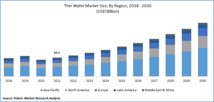
The global thin wafer market was valued at USD 10.2 billion in 2021 and is expected to grow at a CAGR of 12.4% during the forecast period. The growing demand for the thin wafer is expected to be driven by the increasing demand for semiconductor devices, the rising adoption of portable devices, and the growing number of consumer electronics devices.
Know more about this report: Download Sample Report
The thin wafer is replacing conventional semiconductor wafers owing to its cost-effectiveness and ability to fit compact devices without hampering its performance. The rising penetration of thin wafers in consumer electronic devices is expected to drive market growth. Additionally, consumer trend towards thinner smartphones and devices with better operation. Such factors are responsible for adopting the thin wafer in the commercial sector, propelling the market growth.
The COVID-19 pandemic had a negative impact on the growth of the market. Negligible operations across commercial and industrial sector due to a lack of raw material and skilled labor has severely impacted the market. In addition, many manufacturing units were standstill owing to the global lockdown, and less consumer expenditure on consumer wearables and devices such as smartphones, tv, and smartwatches also hampered the market growth.
Thin wafer has a massive demand in the semiconductor and electronic market and has maximum wafer size for many end-use applications. But this wafer cannot absorb a high wavelength with less than 50 mm thickness; such a factor results in inefficiency in thin wafers, and manufacturers look for alternatives with better performance and low power consumption, ultimately restraining the market.
 Know more about this report: Download Sample Report
Industry Dynamics
Growth Drivers
The increasing penetration of electrification and automation technologies in the automotive industry to reduce emissions and improve the efficiency of the vehicle is expected to increase the demand for the thin wafer in this sector. In addition, the growing adoption of electric vehicles across developing nations due to the reduction of fossil fuels also supports market growth. Furthermore, the development of the charging infrastructure of electric vehicles and features such as anti-lock braking, advanced driving assistance systems, and many more require a thin wafer as a semiconductor, boosting the market growth.
Moreover, government entities of many developing and developed nations are heavily investing in producing thin wafer semiconductors. The rising R&D investment and collaboration of key players have also contributed to the development of semiconductors. For instance, the government of Germany has invested around 3 billion euros in reclaiming the semiconductor production sites. This investment is due to the rising demand for semiconductors by industry 4.0 and IoTs, and the production units enhance the access to sufficient microchips to cope with the emerging trends; such factors drive market growth.
Report Segmentation
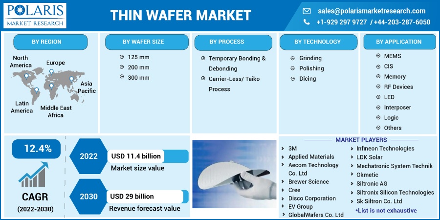
The market is primarily segmented based on wafer size, process, technology, application, and region.
| By Wafer Size | By Process | By Technology | By Application | By Region |
|
|
|
|
|
Know more about this report: Download Sample Report
300mm wafer size segment accounted for the largest share in 2021
300 mm thin wafer segment accounted for the highest revenue share in 2021 owing to its high performance in LED applications. The growing demand for advanced semiconductor products has shifted manufacturer focus to choose larger wafer sizes to build better-outsourced semiconductor assembly and test (OSAT) and foundry (FABs). In addition, rising demand from the solar energy sector for this product also supports market growth.
Moreover, the cost benefits associated with 300 mm wafer size are quite high as compared to other sizes, as they provide profit after assembling and producing semiconductor chips as compared to others. Many key players are highly investing in the production of semiconductor chips of 300mm. For instance, Texas Instruments began initial chip production with a 300 mm analog wafer fab in Richardson and produced millions of analog chips; such factors are essential in driving the market.
Temporary bonding and debonding are expected to spearhead the market growth
The demand for temporary bonding and debonding is expected to spearhead the market growth as it provides mechanical support to the wafers and is also helpful in handling thin and fragile substances. In addition, this process has a huge demand in 3D packaging solutions due to its high flexibility, assembly, and simplification of design and functionality, driving the segment growth.
Furthermore, the process handles stress and helps in the miniaturization of conformity and thickness of the semiconductor, which meets the design demand for IoTs, automatic vehicles, and virtual reality; such factors complement the market growth.
Dicing Technology is expected to witness faster growth
The demand for wafer dicing is expected to surge significantly over the forecast period owing to its smaller design and production of affordable devices for end-use applications. The growing demand for high-density electronics and the development of manufacturing techniques are also expected to drive segmental growth.
Additionally, the emerging trend to pack more computing power in small packages and create innovative, affordable devices for memory, sensor, and smart devices is projected to boost the market over the forecast period. Moreover, key players focus on innovating dicing equipment with high-speed dicing and superior breakage strength. For instance, SR corporation develops next-generation saws. It makes compact and smaller devices and supplies these devices to different sectors, which are helpful in packaging and glass in semiconductor production.
LED segment is expected to account for the largest share in 2030
LED application is expected to dominate the market over the forecast period owing to the rising consumer shift towards LED lightning. in addition, thin wafers provide better electrical benefits and conductivity to LED chips and allow optimal utilization while performing, which has better industrial and commercial use which is expected to bolster the market growth.
Furthermore, thin wafers offer effective temperature management and enhanced LED performance, increasing the demand for the development of various devices. Moreover, the rising adoption of IoT and microprocessors has led to increasing demand for LEDs in the automation sector which is expected to propel the market over the forecast period.
Asia Pacific is expected to proliferate over the forecast period
Asia Pacific is the largest region for thin wafers and is expected to witness faster growth over the forecast period owing to the rising demand for electronic items such as smartphones, tablets, and smartwatches in developing countries of this region. Additionally, with the increasing adoption of electronics, device manufacturers have accepted the latest technological trend to develop high-end consumer devices, eventually boosting the use of thin wafers in the region. Moreover, technological advancement with low labor costs for producing thin wafers across emerging nations also supports market growth.
North America is also anticipated to contribute to the market's revenue growth owing to the well-established fabrication plants and many semiconductor companies. In addition, rising demand for image sensors, RF devices, and LEDs across Canada and the U.S. is expected to drive market growth. Furthermore, the growing adoption of manufacturers to use advanced technologies to develop wafer chips also supports market growth.
Competitive Insight
Some of the major players operating in the global market include 3M, Applied Materials, Aecom Technology Co. Ltd, Brewer Science, Cree, Disco Corporation, EV Group, GlobalWafers Co. Ltd, Infineon Technologies, LDK Solar, Mechatronic System Technik, Okmetic, PV Crystalox Solar PLC, Shanghai Simgui Technology Co. Ltd, Shin-Etsu Chemical Co. Ltd, Silicon Valley Microelectronics, Siltronic AG, Siltronix Silicon Technologies, Sk Siltron Co. Ltd, Soitec, ST Microelectronics, SUMCO Corporation, SUSS Microtec, Synova, UMC, UniversityWafer, Inc., Virginia Semiconductor Inc., VTT, Wafer Works Corporation, and Wafer World Inc.
Recent Developments
In January 2024, Infineon Technologies and SK Siltron CSS confirmed a long-term silicon carbide (SiC) supply agreement to strengthen material availability for power semiconductor applications.
In September 2023, Shin-Etsu Chemical expanded its QST substrate business to support growing demand for GaN power device manufacturing.
In October 2022, Shin-Etsu Chemical Co., Ltd developed the first silicon film-forming emulsion for fiber treatment application. This product can be used as a binder in medical and top coat agents for resin-molded products.
In July 2022, Infineon technologies collaborated with Oxford Ionics to develop high-performance and fully integrated quantum processing units, which are helpful in many industrial solutions.
Thin Wafer Market Report Scope
| Report Attributes | Details |
| Market size value in 2022 | USD 11.4 billion |
| Revenue forecast in 2030 | USD 29 billion |
| CAGR | 12.4% from 2022 - 2030 |
| Base year | 2021 |
| Historical data | 2018 - 2020 |
| Forecast period | 2022 - 2030 |
| Quantitative units | Revenue in USD billion and CAGR from 2022 to 2030 |
| Segments Covered | By Wafer Size, By Process, By Technology, By Application, By Region |
| Regional scope | North America, Europe, Asia Pacific, Latin America; Middle East & Africa |
| Key Companies | 3M, Applied Materials, Aecom Technology Co. Ltd, Brewer Science, Cree, Disco Corporation, EV Group, GlobalWafers Co. Ltd, Infineon Technologies, LDK Solar, Mechatronic System Technik, Okmetic, PV Crystalox Solar PLC, Shanghai Simgui Technology Co. Ltd, Shin-Etsu Chemical Co. Ltd, Silicon Valley Microelectronics, Siltronic AG, Siltronix Silicon Technologies, Sk Siltron Co. Ltd, Soitec, ST Microelectronics, SUMCO Corporation, SUSS Microtec, Synova, UMC, UniversityWafer, Inc., Virginia Semiconductor Inc., VTT, Wafer Works Corporation, and Wafer World Inc. |
FAQ's
The market is projected to reach USD 29 billion by 2030, growing at a robust CAGR of 12.4% during the forecast period.
Key drivers include increasing electrification and automation in the automotive sector, rising EV adoption, growing semiconductor demand, government R&D investments in semiconductor production, and expanding IoT and Industry 4.0 applications.
Dicing technology is expected to witness the fastest growth, driven by demand for high-density electronics, smaller device packaging, and innovations in memory, sensor, and smart device manufacturing during the forecast period.
LED is expected to dominate by 2030, followed by MEMS, CIS, memory, RF devices, interposer, and logic applications, driven by rising consumer shift towards LED lighting and IoT-driven automation adoption.
Asia Pacific is the largest region and expected to grow fastest, driven by rising demand for smartphones, tablets, and smartwatches, increasing electronics adoption, and low labor costs across emerging nations like China and India.
Download Sample Report of Thin Wafer Market
Please fill out the form to request a customized copy of the research report.
